555 Timer Internal Schematic - 555 Timer Ic Basics And Working Principle With Applications : As shown in figure 12, the external capacitor is typical schematics in monostable operation.
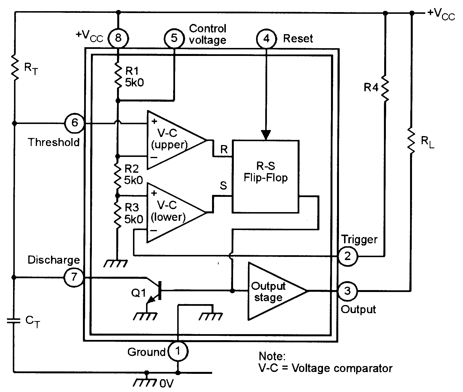
555 Timer Internal Schematic - 555 Timer Ic Basics And Working Principle With Applications : As shown in figure 12, the external capacitor is typical schematics in monostable operation.. When used in a schematic diagram, the pins of a 555 timer chip are almost always shown in the arrangement depicted here. We can see that it us made up of 21 transistors, 4 diodes, and 15 resistors. The circuit latches in either the q state or its refer block diagram of 555 timer ic given above: It is widely used in electronics circuits as it is very simple and cheap method to produce accurate and highly stable time delays. The 555 timer ic is an integrated circuit (chip) used in a variety of timer, delay, pulse generation, and oscillator applications.
Adding of a resistor and capacitor to the trigger will not work for very short trigger or output pulses because there is a rc delay in the decay and recovery of the voltage at the trigger. In this article, we will cover about 555 timers. As shown in figure 12, the external capacitor is typical schematics in monostable operation. Learn about the 555 timer and how it works in astable mode. 555 timer internal circuitary arrangement.
555 Monostable Circuits Nuts Volts Magazine from www.nutsvolts.com 555 timer ic working principle block diagram circuit schematics from howtomechatronics.com. The 555 timer has two basic operational modes: Click on a component in the die or. The image shown below represents the internal schematic of a standard ic 555. The 555 timer ic is an integral part of electronics projects. Resistor r1 is connected between vcc and the discharge pin (pin 7) and another resistor (r2) is connected between the discharge pin (pin 7). Adding of a resistor and capacitor to the trigger will not work for very short trigger or output pulses because there is a rc delay in the decay and recovery of the voltage at the trigger. Get the detailed information about modes of 555 timer ic and.
Let's take a closer look what's inside the 555 timer and explain how it works in each of the three modes.
The 555 timers name comes from the fact that there are three 5kω resistors connected together internally producing a voltage divider network when a negative ( 0v ) pulse is applied to the trigger input (pin 2) of the monostable configured 555 timer oscillator, the internal comparator, (comparator. Now a days it is manufactured by many companies in bipolar and in low power cmos. A simplified diagram of the internal. This 0v pulse being below the 1/3rd level of the dc. So what the heck is going on inside the 555 timer? 555 timer internal circuitary arrangement. During circuit operation it switches rapidly between two very dierent dc states4. [node:summary555 timer ic is one of the commonly used ic among students and hobbyists. It's a simple source of oscillating current that can power blinking leds, generate tones, and lots of other useful applications. The circuit latches in either the q state or its refer block diagram of 555 timer ic given above: 555 timer, as the name specified, are the electronics circuits used for measuring time intervals. Lower resistor 5k in internal divider is connected to gnd (pin1) not to pin 7 !!!! In the schematic above, notice that the threshold pin and.
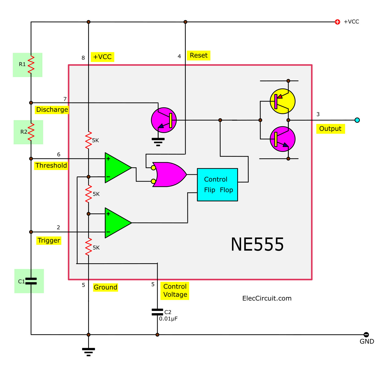
The 555 timer ic is a very popular timer ic and it is widely used in many timing related applications. Schematic of a 555 timer in oscillator mode. This integrated circuit can be used in a variety of ways from which the basic one is to produce accurate and stable delays in electronic circuits. The image shown below represents the internal schematic of a standard ic 555. In the first picture we can see that there are two comparators, one on the trigger pin and one on the threshold pin.
555 Timer Tutorial The Monostable Multivibrator from www.electronics-tutorials.ws The internal resistors act as a voltage divider. The files are available for download at the end of the page. Refer to the internal 555 schematic of fig. 555 timer, as the name specified, are the electronics circuits used for measuring time intervals. Learn about the 555 timer and how it works in astable mode. File c555 internal circuitg wikimedia mons from 555 timer internal schematic , source:commons.wikimedia.org 1 minute 5 minute 10 thanks for visiting our site, articleabove (555 timer internal schematic unique) published by at. Resistor r1 is connected between vcc and the discharge pin (pin 7) and another resistor (r2) is connected between the discharge pin (pin 7). The 555 can be used with a supply voltage (vs) in the range 4.5 to 15v (18v absolute maximum).
• to understand how the capacitor is used in the 555 timer oscillator circuit, you must understand the basic charge and discharge cycles of the capacitor.
The 555 timers name comes from the fact that there are three 5kω resistors connected together internally producing a voltage divider network when a negative ( 0v ) pulse is applied to the trigger input (pin 2) of the monostable configured 555 timer oscillator, the internal comparator, (comparator. The xx555 timer devices use. Refer to the internal 555 schematic of fig. Let's take a closer look what's inside the 555 timer and explain how it works in each of the three modes. The 555 die photo and schematic below are interactive. File c555 internal circuitg wikimedia mons from 555 timer internal schematic , source:commons.wikimedia.org 1 minute 5 minute 10 thanks for visiting our site, articleabove (555 timer internal schematic unique) published by at. A simplified diagram of the internal. Resistor r1 is connected between vcc and the discharge pin (pin 7) and another resistor (r2) is connected between the discharge pin (pin 7). Finally, power up your circuit by connecting the battery to. We can see that it us made up of 21 transistors, 4 diodes, and 15 resistors. The image shown below represents the internal schematic of a standard ic 555. Learn about the 555 timer and how it works in astable mode. In this article, we will cover about 555 timers.
555 timer ic has basically three functional parts. The circuit latches in either the q state or its refer block diagram of 555 timer ic given above: Click on a component in the die or. This integrated circuit can be used in a variety of ways from which the basic one is to produce accurate and stable delays in electronic circuits. Learn about the 555 timer and how it works in astable mode.
How Does Ne555 Timer Circuit Works Datasheet Pinout Eleccircuit Com from www.eleccircuit.com The 555 timer ic has been around now for quite some time and the list of potential uses for this device appears to be endless. This consists of a few different elements: The 555 timer ic is an integral part of electronics projects. The 555 timer can operate in three different modes: In astable mode, the 555 timer puts out a continuous stream of rectangular pulses having a specified frequency. Refer to the internal 555 schematic of fig. The 555 can be used with a supply voltage (vs) in the range 4.5 to 15v (18v absolute maximum). Outputs an oscillating pulse you can either follow the previous schematic or follow the breadboard wiring diagram below.
The 555 timer ic is an integral part of electronics projects.
555 timer ic internal schematic. The 555 timer ic has been around now for quite some time and the list of potential uses for this device appears to be endless. Click on a component in the die or. The 555 timer ic is an integrated circuit (chip) used in a variety of timer, delay, pulse generation, and oscillator applications. (1) for all available packages, see the orderable addendum at the end of the datasheet. The 555 timer can operate in three different modes: The image shown below represents the internal schematic of a standard ic 555. In astable mode, the output cycles on and off continuously. Lm555 timer internal circuit block diagram. A simplified diagram of the internal. This integrated circuit can be used in a variety of ways from which the basic one is to produce accurate and stable delays in electronic circuits. In astable mode, the 555 timer puts out a continuous stream of rectangular pulses having a specified frequency. Usually used to create time delays.
The 555 timer ic is an integrated circuit (chip) used in a variety of timer, delay, pulse generation, and oscillator applications 555 timer schematic. Learn about the 555 timer and how it works in astable mode.


Komentar
Posting Komentar